Miller
Direct Digital Synthesizer ROM Design
Dept.of Elec. and Comp. Engineering
University of Maine, Orono.
ECE 498, “Intro to VLSI Design”–Spring 2006
Designed by
Cyrus Miller
May 2006

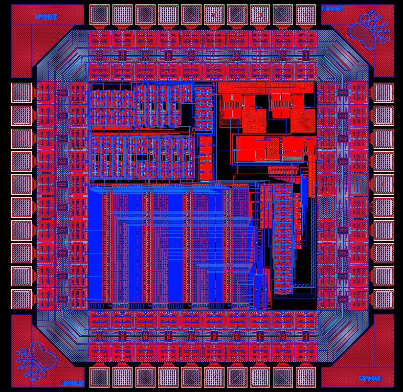
My portion of the classes Direct Digital Synthesizer was to design and lay out the Read-Only Memory that stores the sinusoid information. I worked closely with Anusha Ramanujam in doing this project. In this design, the ROM is given 8 inputs from the accumulator. Those 8 bits allow us to access one of 256 rows of memory, thereby giving us a 256 bit ROM. The ROM stores all of the data that will be needed to create a sinusoidal input; we output this data in 10 bit rows to the DAC. The DAC outputs the sinusoidal voltage level to the output pad of the chip.
My personal chip is unique in that it has both DAC designs, giving two separate outputs. One DAC design consists of a 12 bit ladder and a 3 stage Op-Amp, designed by Steven Fortune. The other DAC design consists of a 10 bit ladder with a 2 stage Op-Amp, designed by Raghu Tumati.
Detailed Explanation: The accumulator was designed by Aravind Reghu and is a 12-bit accumulator operating at a clock speed of 50 MegaHertz. It outputs the 8 bits to the ROM, of which the 6 Least Significant Bits are sent to each of the four 64-bit ROM’s. Splitting the ROM into four separate sections helps both in minimizing capacitance and taking up less space on the chip. Each of the four ROM’s output for every clock cycle– their outputs go to a two stage multiplexer that utilizes the two Most Significant Bits to choose which ROM should be accessed. The final MUX outputs 10 bits to the DAC’s. Each DAC converts this digital signal to a voltage level and the output, at 25 MegaHertz, is sent to two separate pins on the chip.
Complete project details are available in the project report (PDF).
