Record
RF Energy Harvesting Circuits
A project for ECE 547 “VLSI Design”
Fall Semester 2011
Dept. of Electrical and Computer Engineering
University of Maine
Design by
Joseph Record
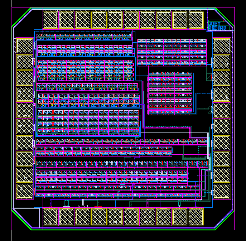
This project presents the design and simulation of various energy harvester circuits. The overall design consists of six different “voltage doubler” configurations. From the six configurations, 14 independent energy harvester circuits have been designed, each consisting of various series connections of the voltage doublers. Multiple RF harvesters were designed to determine the effect of component value and size. The cascaded voltage doulber circuits rectify the full-wave peak-to-peak voltage of an incoming RF signal to produce a DC voltage, ideal for low power sensors networks or other embedded devices. Simulations with a 150 mV 90 MHz input signal indicate an average output voltage of approximately 1.75 V over a 100 us time scale for 20 cascaded voltage doublers. This corresponds to a gain of roughly 11.5 V/V. Cascading more voltage doublers is shown to increase this gain. Test and verification procedures are outlined and described.
The project report (PDF) contains a description of the project and details of the design and layout.
Fall 2011